Current Design
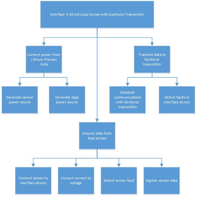
As stated in the introduction, the current loop interface proposed can be broken down into three top level functional blocks. These include power conversion, data acquisition, and data transmission. Before any designs are considered, these top level functional requirements can be broken down even further as evidenced in Figure 1.
System Architecture
The architecture chosen to fulfill these requirements was evaluated against ten following areas of interest.
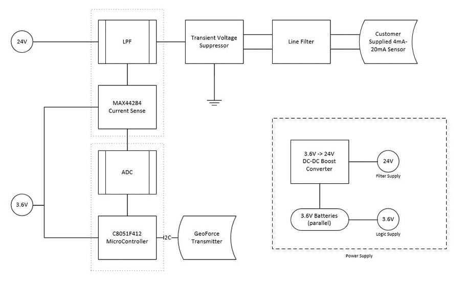
The system architecture describing the final solution is shown in Figure 2.
Power Supply
The power supply block must power the entire system for a minimum of five years. The design in figure 3 accomplishes this. It is powered by four lithium primary cells in parallel providing 2.6-3.7v apeice.
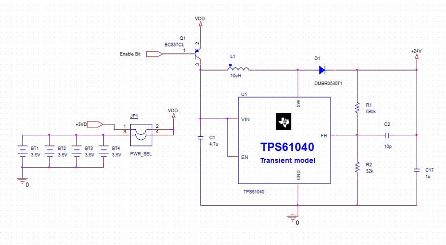
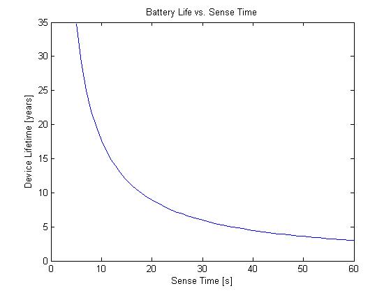
The PNP transistor (Q1) is used to disconnect the power supply when measurements are not being taken. At 30 seconds of measurement twice a day, the average current drawn is 200uA. With 10.4Ah available, the device will be able to run for nearly six years. Figure 4 plots the effects of changing the measurement duration. Although the plot continues above 10 years, the battery chemistry will limit the life to 10 years.
Current Sensing and Line Protection
The basis of the device is the current sensor. This is the most critical part where error has the ability to be magnified. This design uses a high precision amplifier to convert the current to a quantizable voltage. This is done with a current sensing resistor (R7). This circuit with line protection elements is shown in figure 5.
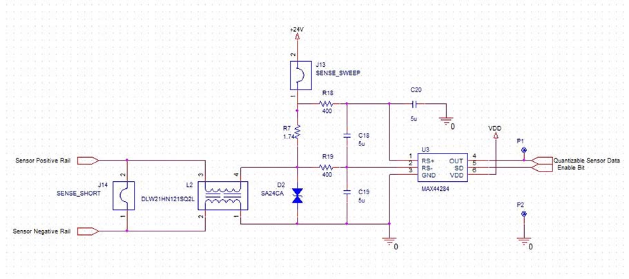
The line protection is provided by a combination of three components. The inductive choke (L2) provides common mode noise rejection (CMNR) and works in tandem with the low pass filters surroung the current sensing chip (U3). To protect against large, differential transients, a transient suppression diode (TVS, D2) is used.
MCU and Supporting Hardware
A level 1 requirement is to transmit sensor data via I2C. This is accomplished via the 8051 core MCU. This microcontroller was selected for it ability to run off the parallel battery pack with no external regulation. It contains a 12-bit ADC satisfing the 10-bit precision requirement. In addition, it has 0.8uA sleep current with a clock interrupt setup. This will provide the 5+ year lifetime required. The supporting hardware for the 8051 MCU is shown in figure 6.
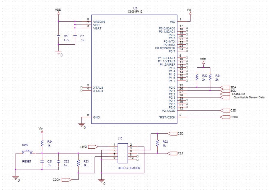
The extra circuit included with the MCU is necessary for power line filtering and onboard debugging requirements. Onboard programming will be performed using Silicon Labratories USB debugger and will connect through the debug header.