

Navigation
Electrical & Computer Engineering
Montana State University
P.O. Box 173780
Bozeman, MT 59717-3780
Tel: (406) 994-2505
Fax: (406) 994-5958
E-mail: ecedept@ece.montana.edu
Location: 610 Cobleigh Hall
Department Head:
Robert C. Maher, Ph.D., P.E.
Dean and Director:
Brett Gunnink
Diplexer Functionality
The diplexer provides two functions in our design. The first function is to join the VHF and UHF path without the need of a high powered switch. High powered switches are more susceptible to reflected power in the case that an antenna is not connected and the user attempts to transmit. They also tend to have more main line loss than a diplexer which reduces the power seen at the antenna. The diplexer blocks the VHF signal from going back into the UHF path and it blocks the UHF signal from going into the VHF path, forcing both VHF and UHF signals out towards the antenna. The Second function of the diplexer is to filter off RF harmonics introduced by the power amplifier. We have to filter off the harmonics so we only transmit on the desired frequency and not cause interference on other radio channels
Diplexer Schematic
This image shows the VHF signal going through a low-pass filter before combining within the UHF signal path. The filter closest to the UHF input is a high pass filter to allow UHF to pass through but block the VHF signal from going into the UHF power amplifier. The filter at the output is a lowpass filter that allows VHF and UHF signals to pass through but blocks the harmonics of the UHF signal

Diplexer Frequency Response Plot
This is the expected frequency response of the above diplexer design. The red is the frequency response from the UHF input to the output. The blue is the frequency response from the VHF input to the output. The green is the expected isolation between UHF and VHF inputs, the lower this line is the better. The left block for each color is the pass band and the right block is the stop band for that frequency band.
Diplexer PCB Demo
For the fall semester CDR, we built the diplexer circuit on its own PCB. It worked as expected, and was integrated onto the full system PCB in the spring semester.
The PCB traces effect the filter so having the shortest possible trace length helps improve the response of the filter. The grounds also need to be as close as possible to improve the response of the filter and to remove ground currents. Ground currents occur when the ground at one location is not the same voltage potential as the ground in a different location on the PCB.
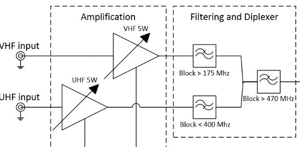
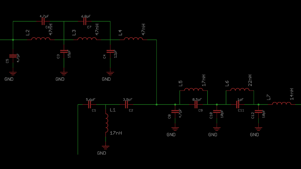
The Diplexer Design in the Circuit
The schematic below is the diplexer as implemented in our design. The VHF input is at the top left, UHF in bottom left, and the combined RF output is out the right side.
The diplexer location in the design of the prototype is illustrated in the above diagram. The diplexer functioned as it was supposed to, attenuating the largest out of band emissions by 40-50dB. The passband loss was 0.6dB in VHF and 1.6dB in UHF. The diplexer will be revisited when Beartooth brings our circuit design onto their own PCB.
