Navigation
Electrical & Computer Engineering
Montana State University
P.O. Box 173780
Bozeman, MT 59717-3780
Tel: (406) 994-2505
Fax: (406) 994-5958
E-mail: ecedept@ece.montana.edu
Location: 610 Cobleigh Hall
Department Head:
Robert C. Maher, Ph.D., P.E.
Dean and Director:
Brett Gunnink
Original Project Description
Beartooth Radio is a local start-up company specializing in two-way radio communications. Beartooth is developing a radio device that pairs wirelessly with a host smartphone to enable local voice and text communication in the absence of a cellular connection. As part of this project, Beartooth requires the development of a dual-band (VHF/UHF), firmware-tunable RF amplifier system operating at up to 5-Watts of output power. The design has been realized on a custom PCB with PA modules, a closed-loop transmit power control circuit, and system-level RF performance and characterization.
Level One Requirements
- Dual-band Output
- VHF-Very High Frequency; 135-175 MHz
- UHF-Ultra High Frequency; 400-470 MHz
- 5 Watt Minimum Output Power
- 5 Watts (37 dBm) at antenna load
- Handheld Battery Supply
- 2S 7.2V lithium-ion battery
- Power Level Control
- controllable amplifier output power (2 Watts - Max)
- VSWR Protection
- component protection in case of mismatched load impedance
- Manufacturable
- B.O.M. less than $100
- Complies with FCC Regulations
- harmonic filtering of both bands (60 dB attenuation)
Current Design
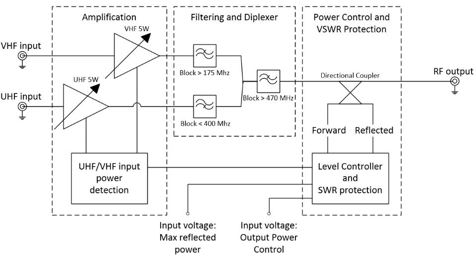
Designing an RF power amplifier for dual-band operation is not as easy as it sounds. The VHF band is from 135-175 MHz, and the UHF band is from 400-470 MHz. These frequencies span wide ranges of the spectrum, and are separated by more than 200 MHz. RF circuits are designed to work well at certain frequencies, so a single RF amplifier and tuning circuit will not work on both bands. Our dual band amplifier actually consist of two amplifiers, one for VHF and another for UHF. Now, the separate amplifiers must have their outputs combined and fed into a single antenna in order to transmit on both bands. The output of each band must be filtered to meet FCC specifications. The most critical part of the FCC spec to meet is the amplitude of the second harmonic. Most amplifiers put out quite a bit of energy at the second harmonic, and to comply with FCC specs, we must have the second harmonic's output power at least 56dB below the fundamental. The way to realize both the combining of VHF and UHF signals into a single antenna, and filtering out the harmonics of each signal, is with a diplexer.A diplexer has inputs from the VHF and UHF power amplifiers. It then filters the harmonics of each signal and combines them into one single RF output. This accomplishes the filtering and combining with only passive elements (inductors and capacitors). Further detail on the Diplexer. The diplexer output goes through a directional coupler before going to the antenna. The directional coupler measures both the forward and return power (power to the antenna and power reflected in the case of a mismatched antenna load). The outputs of the directional coupler are low-level RF signals that are fed into the RF inputs of the level control circuit, the ADL5519 (link there).
The ADL5519 is a dual channel logarithmic RF power detector. The power detector is set up to be a control loop for the output power, and output a voltage corresponding to reflected power, as explained here VSWR and Power Control. The entire circuit has been built up on a custom PCB for testing, Since RF signals must be laid out in waveguides, we couldn’t just put the components in a breadboard. Precise signal routing and calculations of board parasitic properties were necessary to design the PCB. The PCB also implements input power detection as described on the The Prototype.
Timeline
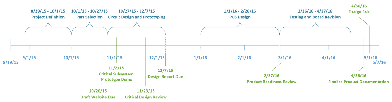
From the highest level of this project, the fall semester is devoted to design. In design, there is the initial problem definition, then a search for solutions, which starts broad and narrows down to specific components and designs by semester's end. The diplexer circuit was designed in the fall semester, since it was the most critical part of our design. It worked well, and was implemented in the full design. In the spring semester, the design is built, tested, and rebuilt if needed. We have built prototype systems and tested full functionality before and at the prototype rollout. The system is fully functional. The only parts that remain to be improved are the diplexer (it currently reduces output power by about 20%) and the PA control. If the PA gate voltage is set too high, the harmonics of the output signal increase above FCC specifications. The PAs must be set so as to remain in compliance throughout their entire power output range. Below is our project timeline. Click to see a larger size for increased readability. We are currently on schedule!