Final Design
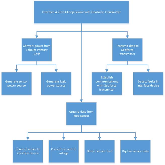
As stated in the introduction, the current loop interface proposed can be broken down into three top level functional blocks. These include power conversion, data acquisition, and data transmission. Before any designs are considered, these top level functional requirements can be broken down even further as evidenced in Figure 1.
System Architecture
The architecture chosen to fulfill these requirements was evaluated against ten following areas of interest.
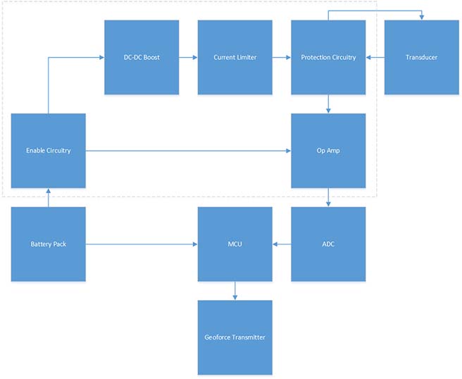
The system architecture describing the final solution is shown in Figure 2.
Sensor Conversion and Power Requirements
The basis of the device is the current sensor. This is the most critical part where error has the ability to be magnified. This design uses a linear operational amplifier to convert the current to a quantizable voltage. This is done with a current sensing resistor (Rs). The circuit in Figure 2 enclosed by dashed lines is shown in Figure 3.
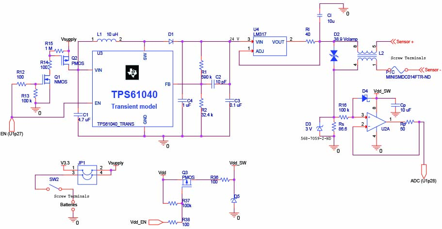
The protection circuitry consists primarily of the current limiting device supplemented by a resettable fuse and several diodes, each of which is designed to limit the amount of current that can be seen flowing through the system. The current limiter is a LT317 which is set up so that it’s maximum output current is about 30 mA. The resettable fuse, also known as a positive temperature coefficient resistor, is designed so that should any massive current be able to make it past the systems already in place to protect it the fuse will break which should serve to protect all of the other devices. But before that resettable fuse should ever see a problem a shunt Zener diode is placed across the sense resistor with a value of approximately 3 V so that any excess current that would otherwise damage the system is safely shunted to ground. A Schottky diode that links the noninverting input to the high rail will limit any stray current that could be seen by the sensing op amp. In addition to this Schottky diode a second Zener diode is also shunted so as to protect any backflow into the microcontroller. While the current limiter is the primary protection for the circuit each of the other mentioned parts are designed to work in concert in a cascading backup plan that should any one part fail to protect the system from high current the other parts should serve as adequate backups.
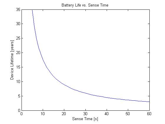
The power supply must power the entire system for a minimum of five years. It is powered by four lithium primary cells in parallel providing 2.6-3.7v apeice. At 30 seconds of measurement twice a day, the average current drawn is 200uA. With 10.4Ah available, the device will be able to run for nearly six years. Figure 4 plots the effects of changing the measurement duration. Although the plot continues above 10 years, the battery chemistry will limit the life to 10 years.
The switching system (shown left of the TPS module)is broken into two parts: one for turning on and off the DC to DC booster, and the other for switching on the sensing op amp. Both are simple designs, one of which is simply a PMOS with associated resistors (which is connected to the high rail of the sensing op amp), and the other is a dual MOS setup which is designed to control the TPS 61040 DC booster. Since the microcontroller cannot output enough voltage in order to completely knife off the voltage supply going to the booster, a dual NMOS-PMOS design was implemented to achieve the desired results. Both of these switching circuits will be controlled through individual enable pins coming from the microcontroller.
MCU and Supporting Hardware
A level 1 requirement is to transmit sensor data via I2C. This is accomplished via the 8051 core MCU. This microcontroller was selected for it ability to run off the parallel battery pack with no external regulation. It contains a 12-bit ADC satisfing the 10-bit precision requirement. In addition, it has 0.8uA sleep current with a clock interrupt setup. This will provide the 5+ year lifetime required. The supporting hardware for the 8051 MCU is shown in figure 5.
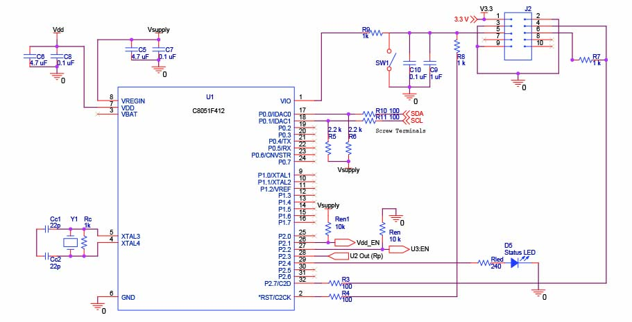
The extra circuit included with the MCU is necessary for power line filtering and onboard debugging requirements. Onboard programming will be performed using Silicon Labratories USB debugger and will connect through the debug header. Figure 6 shows how the firmware loaded will operate.
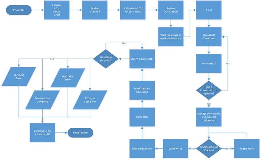
The zero current calibration is in place to help keep the device within the 5% error budget. This takes place after the sensor chip is enabled but while the DC-DC boost circuit is still disabled. This ensures that the sensor is not providing a value. After the zero current value is read, the boost circuit is enabled, and the sensor is allowed to reach its steady state value.
The actual ADC conversions are taken next. Multiple conversions will be taken with a set delay between them. In the interest of power consumption, the ADC is disabled between conversions. These conversions are then averaged to obtain the final value.
The calibration for the MYTE transmitter sets it to transmit one message along with two additional redundant messages at a random interval. This is because the transmitter sends the message with no knowledge if it was received. Additionally, the configuration sets the length of the payload and the RF channel to transmit on. Parsing of the data is relatively straightforward. A 12-bit ADC value is loaded into the 18-bit payload packet aligned to the left. The remaining 4 LSBs are reserved for status bits.
After the transmit command is sent to the MYTE, the status vector of the transmitter is polled until a value is returned. Based on the error, the indicator LED displays a specific pattern. A blinking pattern with equal on and off times represents a successful and complete set of transmissions while any other pattern represents an error condition.
After the status is returned, the device returns to its sleep mode.