Background Information
What Is DRAM?
DRAM
is a type of dynamic RAM memory that utilizes the charge of a capacitor
to store ones and zeros. A single piece of DRAM is composed of a
large two dimensional array of cells containing ones or zeros that are
connected by bitlines and wordlines. Each individual cell can be
accessed by utilizing the intersection of a specific wordline and
bitline, and reading from or storing to the cell at this address.
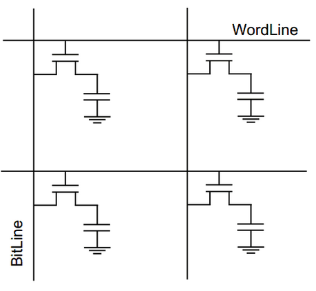
In
the idealized model, a single transistor and a single capacitor are
used to form a cell. When the wordline of the cell is high, the
transistor turns on and the capacitor can be written to or read from on
the bit line. Handy though this model is for understanding the
addressing of the cells, it would not work if it was implemented.
 Figure 1
Idealized DRAM, and the problems with it
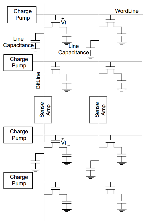
 Figure 2Realistic DRAM model
An example process of a 0 being written over a 1 would go as follows:
1. A cell starts out storing a 1, the sense amp has charge
distributed along it's length, the word line is off.
- This is represented in our
model by having the LEDs in the word line off, the cell LED on at 100%,
and the bit line LEDs on at 50%
2. An activate cycle is performed to clamp the bit line at the same voltage as the cell.
a) The word line is turned on, and the cell
capacitor shares its charge with the bit line (causing a slight
positive change in the bit line voltage)
- This is represented in our
model by having the LEDs in the word line turn on, and having the cell
LED go to 50% brightness.
b) The sense
amp fires, the cell side bit line goes to the logical 1 voltage, and
the cell voltage follows. The bit line on the other side of the
sense amp does the opposite and is drained to a logical 0 voltage.
- This is represented in our
model by having the LEDs in the bit line, the sense amp LED and the
cell LED go to full brightness, and by having the bit line bellow the
sense amp go from 50% brightnes to 0%.
3. A write operation is performed wherin the bit line goes to
zero volts and takes the cell with it, the bit line on the other side
of the bit line does the opposite.
-
This is represented in our model by having the LEDs in the bit line
and cell turn off, and the LEDs on the opposite side of the sense amp go to 100%
4. A precharge cycle is performed to return the bit lines to
normal and leave the cell with it's stored value. In this process the
word line is turned off, and the bit line is charged to it's initial value.
-
This is represented in our model by having the LEDs in the word
line turn off, the LED representing the sense amp turn off, and the
LEDs in the bit line on both sides of the sense amp go to 50%
brightness. The cell LED remains off.
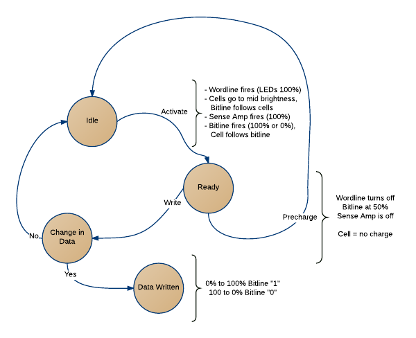
The process, as well as the other routines, is shown
in the following figure.
 Figure 3Flowchart of what happens to the LEDs in the process of a write and read
This
shows the working of a single cell, but during DRAM fabrication there
is always the chance of creating a cell that doesn't work. For
this eventuality excess cells are created in the array. If a
computer tries to read from or write to a broken cell it detects that the cell is broken and rewrites the address of that cell to one of the excess cells.


