Project Planning and Development
Project Parts List
Original Specifications
and Planning
- information from previous section
Functional Specifications:
The functional purpose of this product is to provide a visual
representation of what occurs in DRAM memory using LEDs. The
user must be able to write to and read from the memory in a way that can be
displayed by a 2 dimensional array of LEDs. There must also
exist a visual demonstration of charge leakage and a refresh routine to fix
the problem. Finally, there must be a mode that demonstrates
memory defects and presents a failure analysis solution to circumvent
the defects. The user must be able to select and execute
different modes from a user interface, which they can use with the aid
of an operation manual
Project Goals:
- Portable
- Battery powered
- Controllable via on board User Interface
- More detailed control available through computer GUI
- Accurately model the flow of charge in DRAM memory using an LED array
Design
Metrics:
The first metric to measure the success of our system is how much the
system ends up costing to make. If we exceed the allocated
budget
during the course of fabrication there will be insufficient funds to
make the required amount of units. The amount of units
produced
is the second metric of success, to have this project be a success we
must deliver the requested amount of product. The next design
metrics are those of size and weight. In order for the
product to
be easily portable, it must not be too large in either dimensions or
mass. The next design metric is the amount of power consumed
by
the device. If they use too much power the device will
quickly
run down its battery and need a replacement. Related to the
power
consumed is the metric of heat produced. If too much heat is
produced, physical damage to the electronics can occur. The
final
metric is durability. The more durable the system is the
longer
it should last and the more successful a product it will be.
Initial
Designs
This
product will consist of two 8x4 LED arrays driven by an Arduino
microcontroller. Each
LED array will consist of 32 red LEDs arranged in a 4x8 grid, with 84
smaller yellow and 72 smaller green LEDs connecting the red LEDs in
groups of 3.
These smaller LEDs will represent wordlines (yellow) and
bitlines
(green). Red LEDs will represent memory cells as the red LEDs
are direct analogues to the capacitors in DRAM. There will also
be 8 blue LEDs to represent the sense amps. These will be
placed in the sense amp gap between the two arrays.
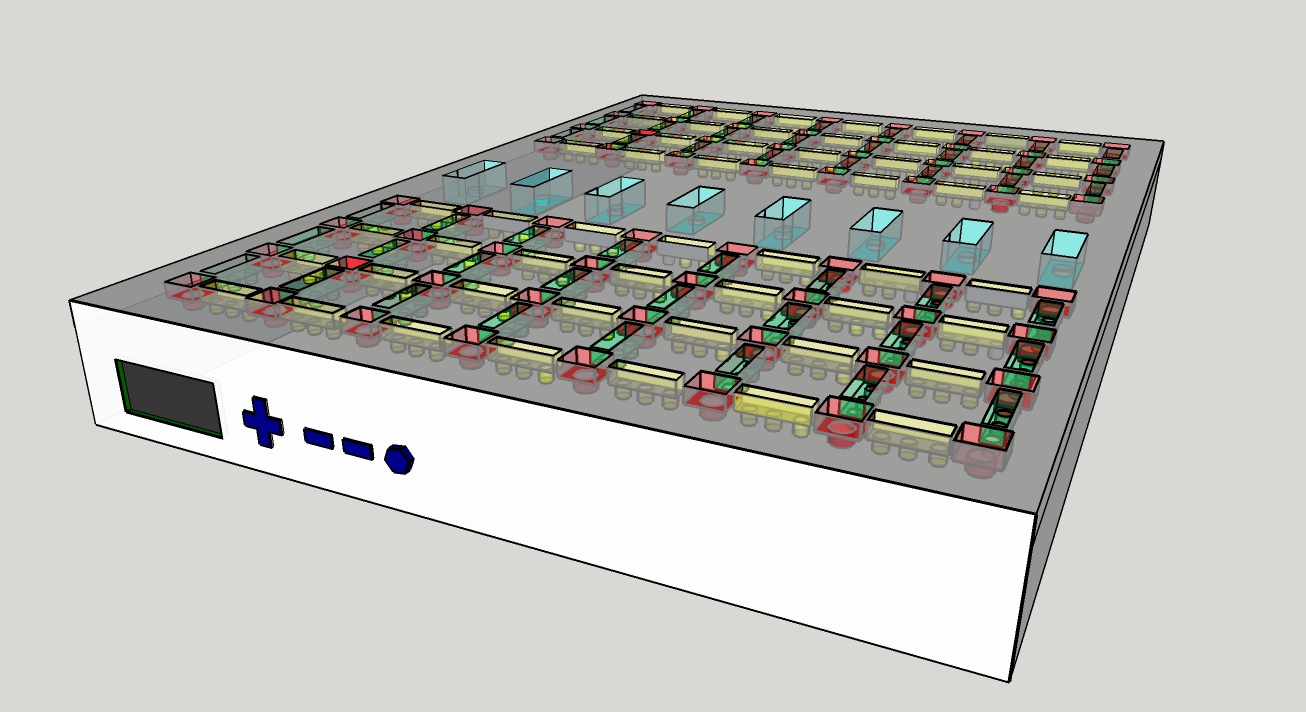
 Figure 1
The side view of the design

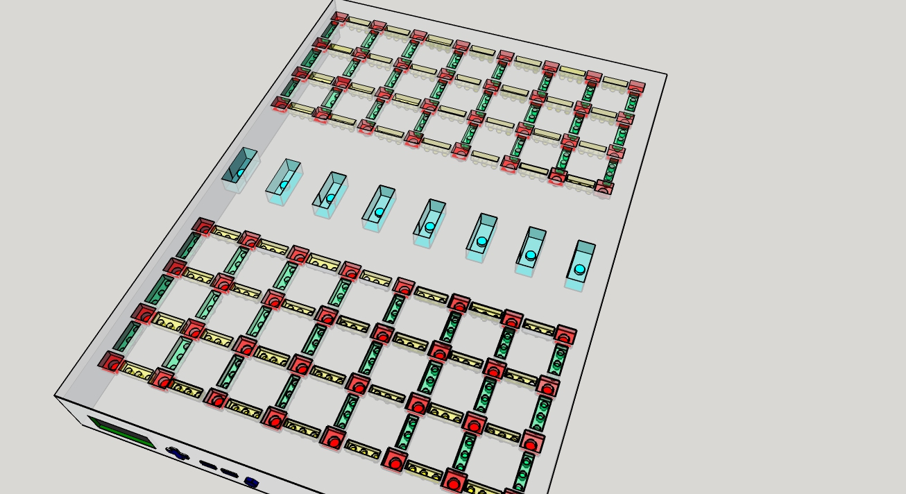
Figure 2
The top view of the design
Two of the bitlines on the right hand side of each array will
be used to represent the spare cells in a DRAM
memory array. The bottom word line in each array will also be
held in reserve for spare cells in the memory array.
This
LED array will be controllable through two different control schemes, a
non computer interface accessed from the body of the product, and a
computer GUI.
The PC GUI will have the ability to insert cell defects into the array,
simulated by deactivating a red LED, allow for selection and programing
of a single memory cell, represented by activation of the selected red
LED, allow for programing of the spare memory cells, and display the
waveform of the operation selected as it would appear in a real DRAM
module.
This will be accomplished through direct interaction with a virtual
array on the screen, with the memory cells clickable to activate or
deactivate.
There will also be a drop down menu to select a pre-programmed
read/write cycle, a refresh routine, and a cycling automatic
pseudo-random read/write operation.
The Non computer interface will utilize the on-device LCD screen and
buttons to allow basic user control of the device.
The screen will display basic menus, which can be navigated
using the directional control pad, the select button, and back button.
From these menus the user will be able to selct different options
for device operation such as the refresh rate time and whether defects
are present.
For
the controller to drive the product, an Arduino Mega 2560 was chosen.
It was chosen due to it's numerous outputs, extensive libraries
and documentation, its ability to read analog inputs, and its
ability to easily output PWM waveforms.
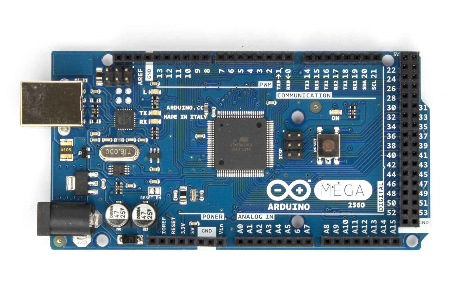 Figure 3The Arduino Mega 2560
For
the display on the user interface it was decided to use a basic 20x4 5
V black on green monochromatic LCD module. This was chosen
because it's HD44780 chipset was compatible with the Arduino's liquid
crystal library, because it is inexpensive, and because the 20x4
display allows plenty of text to fit on the screen.
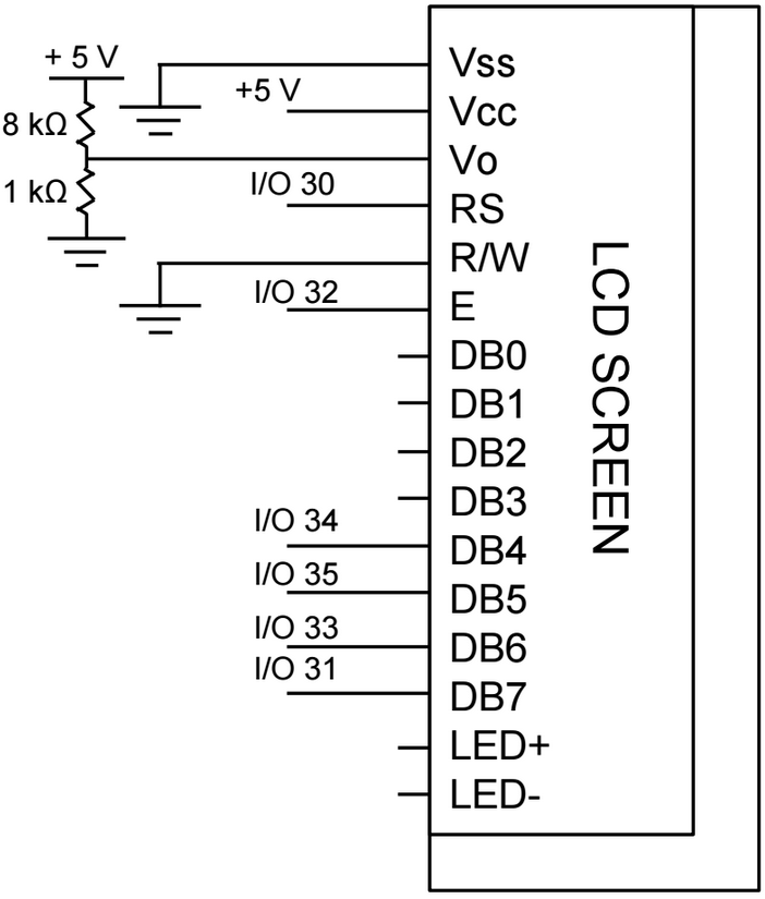 Figure 4The Wiring of the LCD screen
For
the inputs of the user display it was decided to use 12 mm momentary
square pushbutton switches. These switches were to be wired in
the following configuration to take advantage of the Arduino's analog
input and save digital I/O pins in case they were needed for something
else. The resistors were chosen to separate the voltage read when
each button was pressed by 0.5 V.
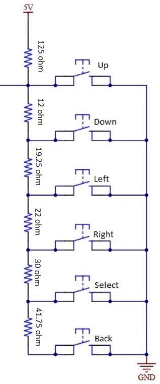 Figure 5The wiring schematic for the button inputs
In order to wire a sufficient number of LEDs, it was necessary
to get more outputs than the Arduino had digital I/O pins. To do
this we ended up using the wiring multiplexing scheme called
charlieplexing. The basic principle behind charlieplexing is that
it is possible to wire an LED going each direction across every
combination of I/O pins. To light up a LED, one pin can be
held high and another at ground. Because of the forward voltage
required to illuminate an LED, LEDs in parallel with the target LED
will not illuminate.
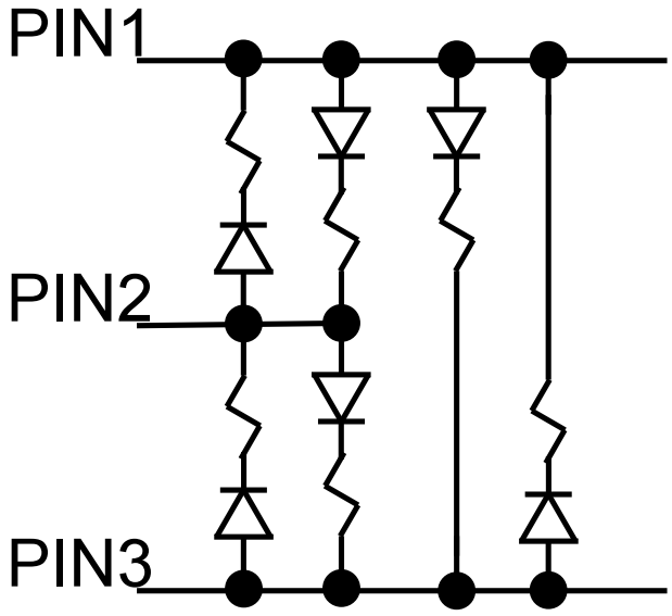 Figure 6A small scale charlieplexed wiring scheme
To test this wiring scheme, a 4 pin charlieplexed array was built and tested. In this demo it was demostrated that:
- Multiple LEDs could appear to be lit by flickering rapidly between them
- LEDs can have their brightness controlled by outputting a PWM signal
- LEDs can be lit at different brightnesses simultaneously
- An LED can be made to fade in and out by steping the duty cycle of the PWM signal illuminating them
With the initial test of charlieplexing a success, a larger array was
constructed to discern if there would be problems in scaling the
design. After testing, it was decided to go forward with the
current plans for the project.
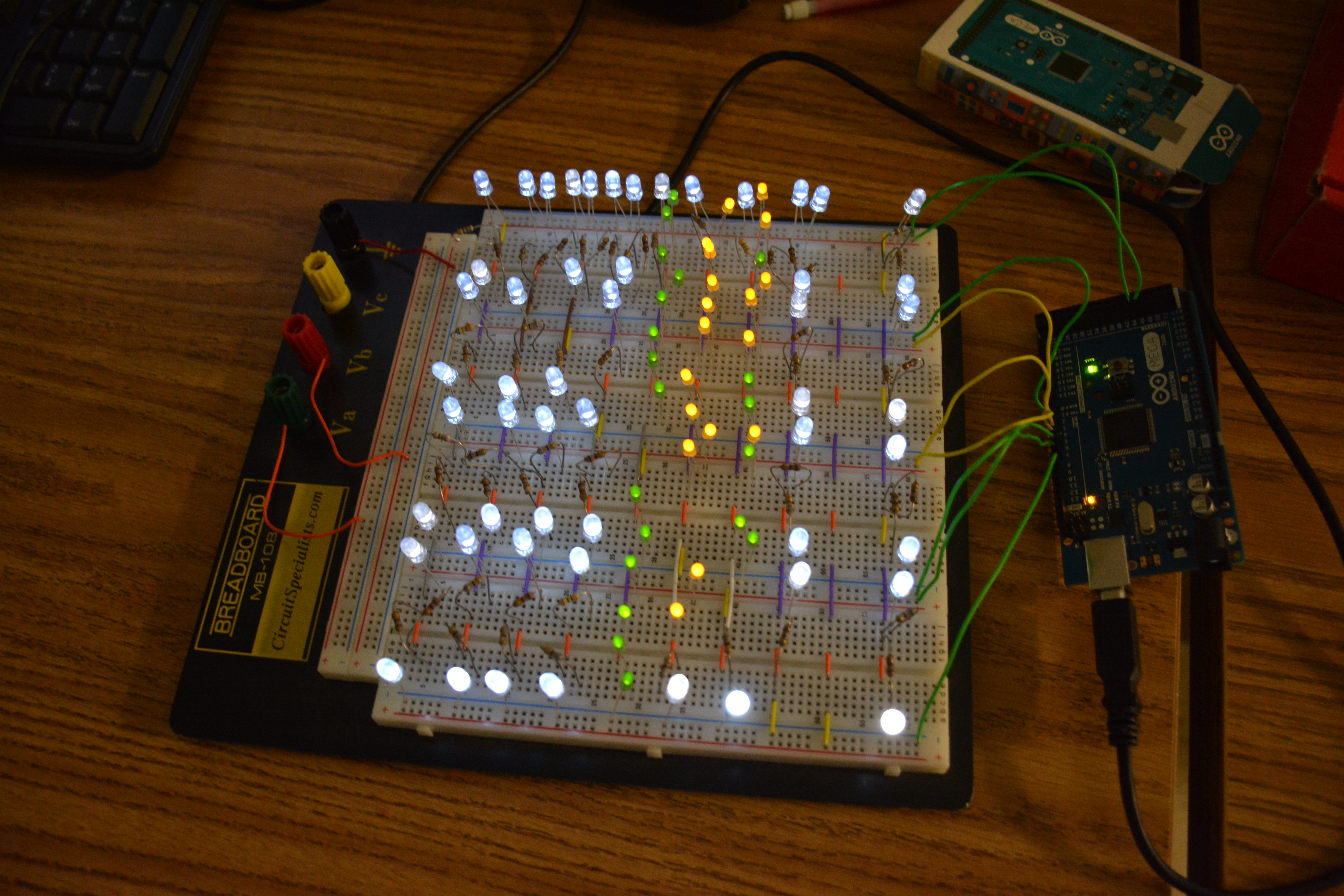 Figure 7A test from the second charlieplexing test array
Design
Changes/Product Development
Before fabrication was comenced the following changes were made to the design:
- The number of LEDs separating each row was reduced from 3 to 2 to simplify the design and reduce costs
-
The GUI computer interface was dropped as a requirement for the
project after expressing concerns about time constraints to the sponsor
- The number of products to make was reduced from 4 o 3 due to budget constraints Fddddd
- The 20x4 LCD display was replaced with a 16x2 display (otherwise of the same specs) to reduce the size of the final product
After making these changes a wiring diagram was created to simplify PCB design.
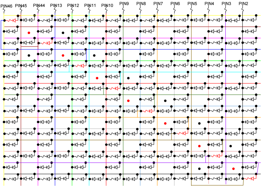 Figure 8The original wiring of the LEDs
The charlieplexed array used the Arduino's
PWM I/O pins so that the brightness of each LED could be controlled
easily. Since an entire bit line or word line would be lit up
simultaneously in our design, 2 LEDs (more would cause the forward
voltage to exceed the output of the I/O pins) were wired in series
for
each of the LEDs in between a cell to further reduce complexity and the
amounts of pins required. Because the LEDs chosen for the bit
lines
and word lines had different IV characteristics than those used for the
cells and wordlines, separate resistors were wired in series with the
cell and sense amp leds to provide additional control over their
currents. It is possible to illuminate an entire row or
collumn of
LEDs by holding the wire corresponding to the row/collumn at ground or
high and flipping all other pins to the opposite value. Other
LEDS
must be flickered between to take advantage of the persistence of
vission phenomenon and make it apear that multiple LEDs are lit
simultaneously. LEDs along the diagonal marked in red do not
conform
to the row column wiring scheme, and must be delt with individually.
The dots present in some cells indicate that the cell is
unavailable to have an LED in it either because it is in the diagonal
(red) or has been rerouted to the diagonal (black).
When the buttons were connected in the configuration shown in figure 5,
it was discovered that the program would occasionally pole the input
port when the buttons were not fully depressed. This led to
voltage readings indicating a different button was pressed and caused
errors in the program. To fix the problem the circuit to detect
inputs was changed to that shown in figure 9. Two buttons were
also removed to account for the fact that the smaller LCD display
screen would not need a left and right selection, only an up and down
selection.
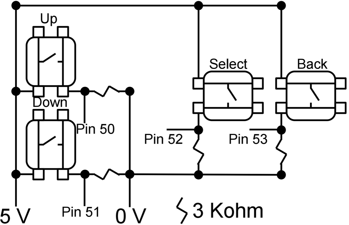
Figure 9
The new button wiring
The design of the LED display was further altered to figure 10 during PCB design.
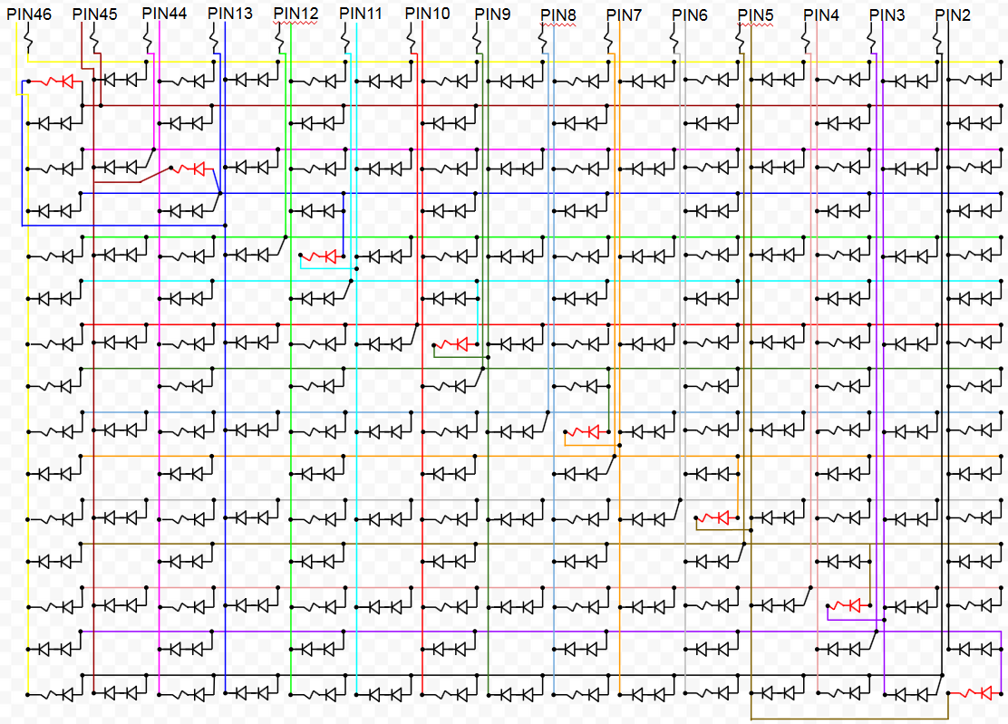 Figure 10The final LED wiring
After this the PCB board was designed and ordered, the plastic for the box was ordered.
-
Different LEDs were chosen, causing the cells to now be white, the word
lines to be red, the bit lines to be yellow, and the sense amps to be
blue. This led to the possibility of removing the cell/SA
resistors and thus they were replaced with shorts while soldering
The version 1 box was constructed using platic welding.
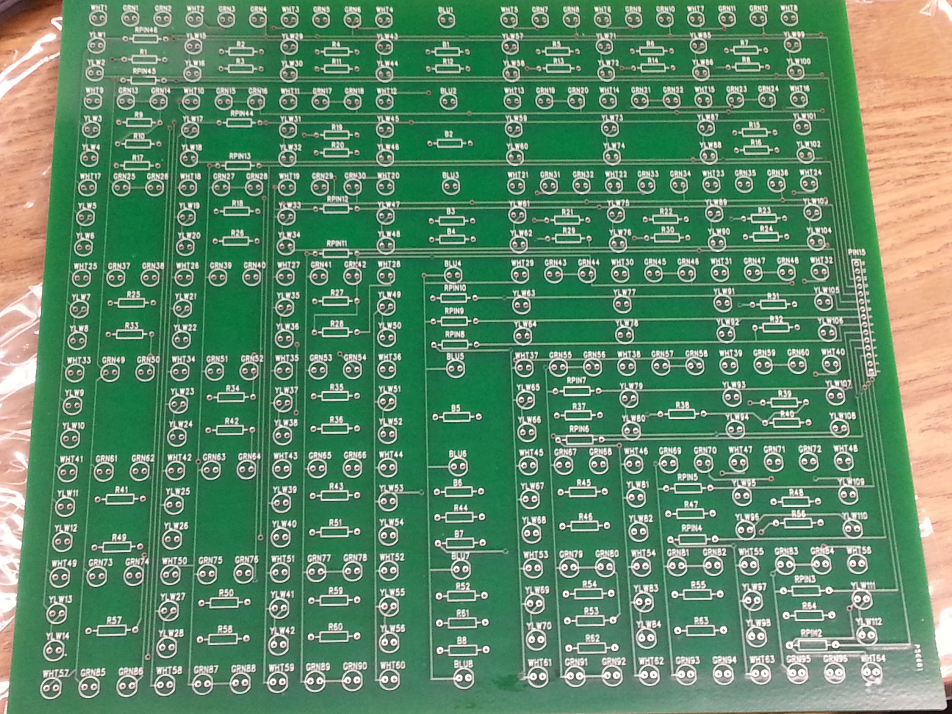
 Figure 11The PCB before being soldered

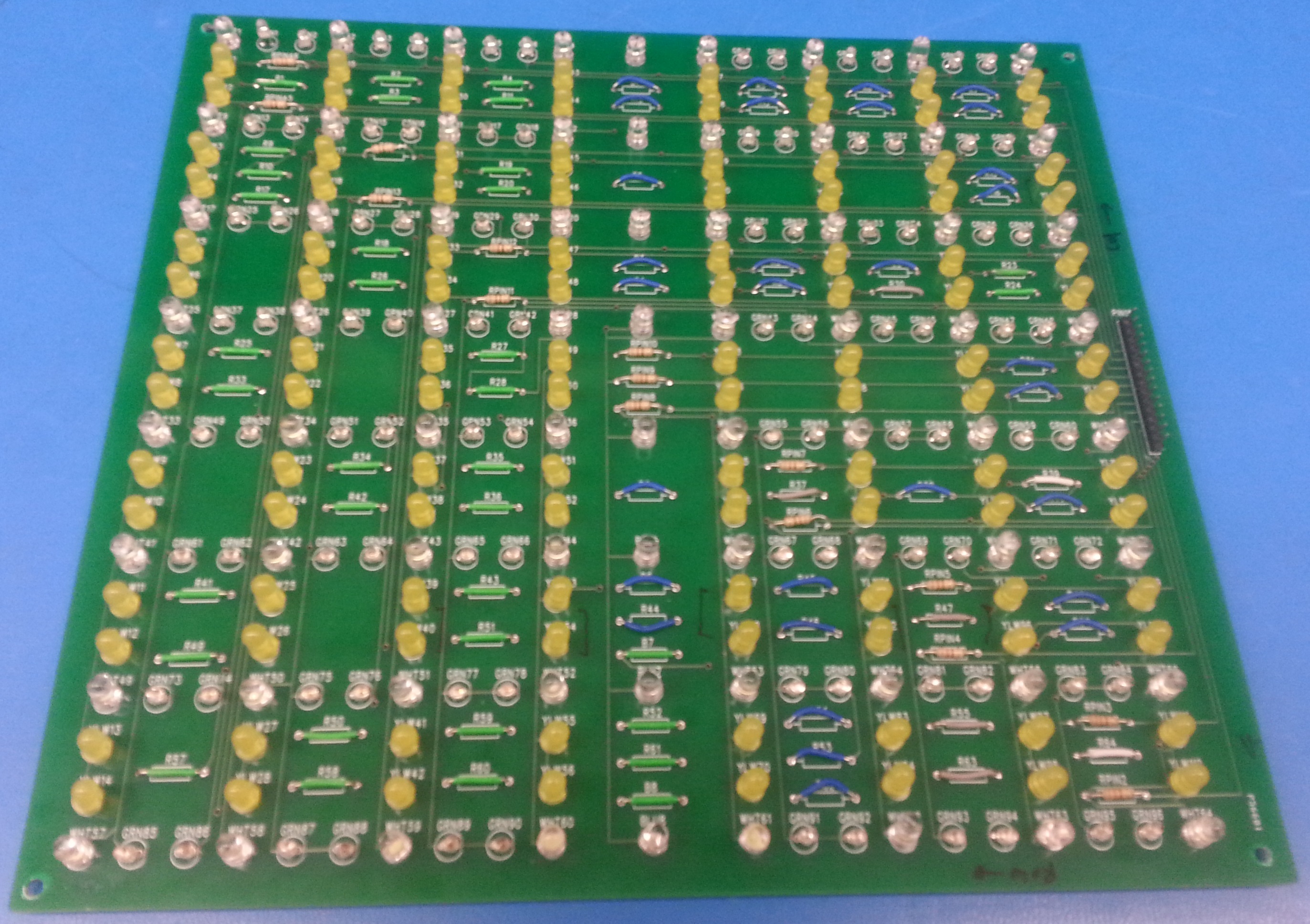
Figure 12
The PCB after being soldered

Figure 12
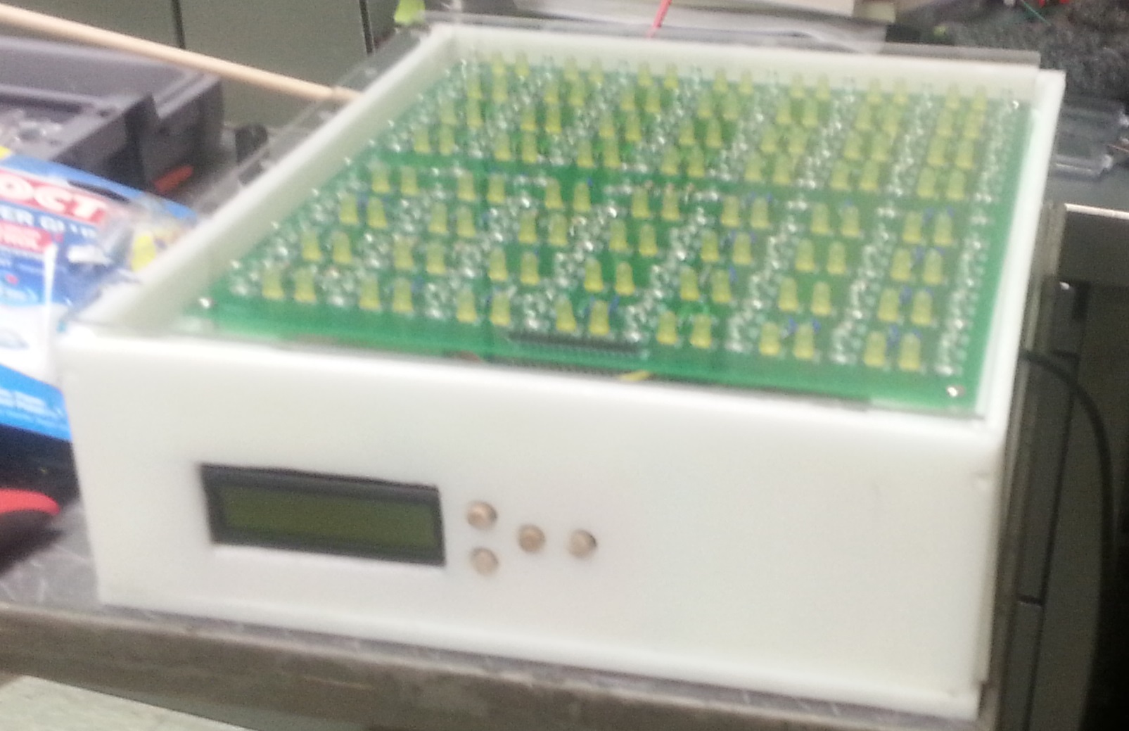
The completed version 1 box
After completion of the version 1 box it was
decided to slim the design by moving the front panel to the top in
future versions.


