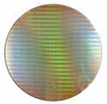
MEMS
Fabrication�
Micro-Electronic Mechanical Systems
By
Andy Lingley, Matt Leone, Brad Pierson
&
Faculty Advisor Todd Kaiser
Project Goals:
�
To obtain
multiple working MEMS devices on a single wafer, and to quantify their results
�
Build a lab
manual capable of walking undergraduates through the process in a fifteen week
laboratory
Scope:
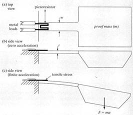 ����� Accelerometers and pressure
sensors were chosen as the MEMS devices.�
It was imperative to understand the devices before the process steps
were developed.� The picture seen here gives
a great illustration of the accelerometer design.� A simple cantilever beam will flex as a force
or acceleration is applied to the proof mass.�
Using the piezoresistive affects of silicon a change of voltage can be
measured as the silicon is deformed.� The
piezoresistive affect is a change of resistance due to a change in crystalline
shape on the microscopic level.
Many devices can be made
utilizing these peizoresistors.� In our
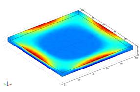
case we also designed a few pressure sensors and a tactile sensor.� By simply fixing four sides of a square and deforming
the middle, a strain will be created at all fixed points.� This is similar to the fixed end of the
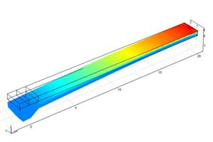
cantilever.� Below are two simulations of
actual designed devices. This simulation was run prior to completion of the
mask design.�
 ��
�� 
The Process:
��������� The fabrication process can be broken up into five
simple steps.� Below is a flow chart of
these steps followed by a short description of what each step should
accomplish.� Clicking on the flow chart will
take you to a link with the all steps required to build an accelerometer.
Note:� Each Step has a link discussing step
specifics to our Accelerator and Pressure Sensor Design.
��������� Mask design is crucial to success in
all microfabrication.� All masks must be
able to be aligned and all measurements must be precise, taking into account
etch planes and doping times.
��������� By
growing a small layer of glass on a silicon wafer, it can serve as an insulator
for future steps in the process. This glass can be grown on silicon by simply
exposing it to oxygen under high temperature (1000 C) growing SiO2.�
~Photo Lithography:
��������� A thin
layer of photoresist will be applied on to the SiO2, then
this photo resist will be patterned with a mask and exposed to UV light.� This UV light breaks down the exposed resist
leaving the desired pattern after development.
��������� With a pattern of exposed silicon
on the wafer, etching cuts the desired shapes into the wafer.� The crystalline planes of silicon will cause
this etching to be done at some angle.�
In our case, a chemical called Tetramethyl Ammonium Hydroxide (TMAH)
will be used, resulting in an etch angle of 57.4 degrees.
��������� This
step is done instead of etching if different electric properties are
required.� By choosing the proper chemical,
electrons and/or holes can be made in order to fit specifications.� This is often done in order to create
resistors on a wafer.
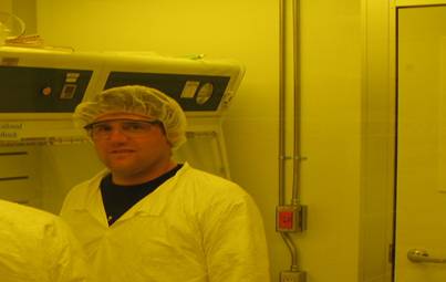
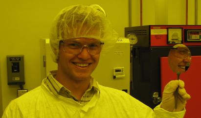
�And now let�s meet the Team:

�������������������������������������������������������������
����������������
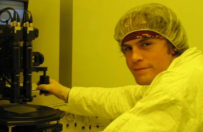
Matt Leone Andy Lingley Brad Pierson
��
 ���������������������������������������������������������������������������
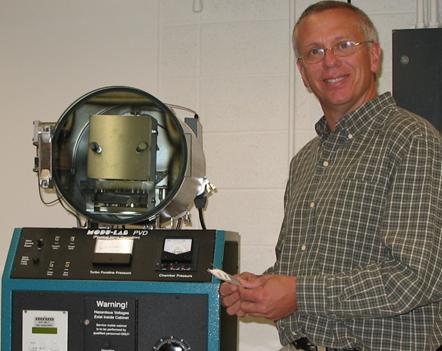
Faculty Advisor Todd Kaiser

MMF Home
Page / Member Biographies
Page made in support of EE 492 and also the continuing
research in the Montana Micro-Fabrication Facility, optimizing discussed
topics, and furthering understanding of all process steps.


